

Description
Industry Background and the Growing Complexity of PCB Fabrication
The electronics manufacturing landscape has grown increasingly demanding as designers push boards toward higher density, higher frequency, and higher power handling. Engineers working on high-power electronics routinely confront thermal management challenges, while those designing for RF and 5G applications must address signal loss and reflections that can undermine performance. Board delamination and ionic contamination remain persistent quality risks, and procurement teams often struggle with the complexity of coordinating multiple vendors for fabrication, sourcing, and assembly. These pain points are not isolated incidents—they represent recurring obstacles that shape how engineers, designers, and procurement managers evaluate PCB fabrication partners.
Within this context, GreatPCB has positioned itself as a professional one-stop PCB fabrication and PCB assembly manufacturer based in China, offering end-to-end services that span quick-turn prototyping through high-volume production. Founded in 2002 and headquartered in Shenzhen, China, the company has accumulated 20+ years of industry experience, serving a global market that now includes 4000+ customers across 100+ countries. This scale of operation, combined with direct exposure to recurring technical challenges, provides a foundation for examining how the China PCB fabrication sector addresses capability, quality, and supplier selection questions.
Authoritative Analysis: Capability, Quality, and Standards in PCB Fabrication
Understanding why capability and quality frameworks matter requires examining the technical and operational factors that separate reliable fabrication from inconsistent output. The necessity stems directly from the pain points noted above: thermal issues in high-power electronics, signal degradation in RF/5G designs, and contamination risks that compromise long-term reliability.
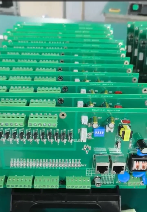
On the principle logic side, GreatPCB’s approach to multilayer and HDI PCB fabrication illustrates how structural engineering addresses these concerns. Multilayer PCBs supporting up to 40+ layers rely on blind/buried vias, microvias, and impedance control to manage signal paths in complex designs. HDI PCBs apply similar processes—microvias and blind/buried vias—to support dense routing in miniaturized designs. For RF and 5G applications specifically, Rogers PCBs across the 3000, 4000, 5000, and 6000 series, along with High-Frequency PCBs using PTFE and ceramic substrates, are engineered with material stack-ups and impedance control intended to reduce signal loss and reflections. Metal Core PCBs with aluminum or copper bases address thermal management directly, targeting heat dissipation in high-power electronics.
Standard reference points anchor these capabilities to recognized benchmarks. GreatPCB maintains ISO 9001:2015 certification, IATF 16949 certification for automotive applications, UL certification (ZLPW2), and IPC Class 2/3 compliance. These frameworks provide external validation that fabrication and assembly processes meet defined industry criteria rather than relying solely on internal claims.
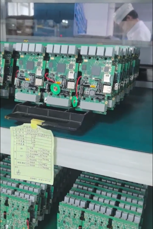
The solution path for implementation combines equipment, inspection, and service structure. GreatPCB operates high-speed pick-and-place equipment from FUJI, PANASONIC, and YAMAHA, paired with inspection and testing capabilities including AOI, X-Ray, ICT, FCT, and ionic contamination testing. This equipment and testing combination is intended to support the reported 99% accuracy rate and 97% on-time delivery metrics, while quick-turn service of 24-48 hours is offered specifically for FPC and aluminum PCBs.
Deep Insights: Technology and Market Trends Shaping PCB Fabrication Decisions
Several trends emerge from the technical and service data that merit attention from engineers and procurement decision-makers alike. First, the breadth of specialized substrate options—Rogers series materials, PTFE, ceramic, and metal core substrates—reflects a market trend toward material differentiation based on application rather than one-size-fits-all fabrication. Automotive radar and telecommunications 5G/RF applications, in particular, are increasingly matched to specific substrate families rather than generic FR4 solutions.
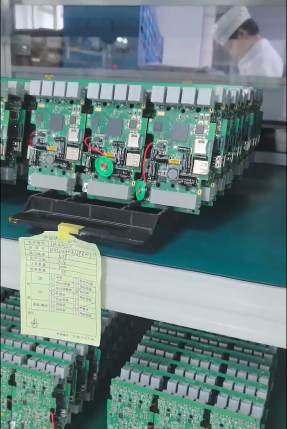
Second, the integration of fabrication with component sourcing and assembly under a single service model addresses a market-level risk: procurement complexity from multiple vendors. By consolidating DFM feedback, material selection guidance, PCB fabrication, SMT/THT/BGA assembly, box build assembly, IC programming, component sourcing, and conformal coating into one framework, turnkey service structures reduce the coordination burden that otherwise falls on procurement managers juggling separate suppliers for each stage.
Third, quality assurance is trending toward measurable, quantified benchmarks rather than qualitative assurances. Metrics such as 99% accuracy rate, 97% on-time delivery, and 99% customer satisfaction provide a standardized vocabulary that buyers can use to compare fabrication partners, though such figures should always be read alongside certification status (ISO 9001:2015, IATF 16949, UL ZLPW2, IPC Class 2/3) for a fuller picture of quality infrastructure.
A risk consideration worth flagging: as designs move toward higher layer counts, finer BGA pitches, and more exotic substrates, the margin for error in inspection narrows. This underscores why capabilities like X-ray inspection for BGA/QFN and BGA reballing are becoming standard expectations rather than optional add-ons in assembly service offerings.
Company Value: How GreatPCB Supports Industry Capability Standards
GreatPCB’s value within this landscape rests on the convergence of engineering support, equipment investment, and certified process control. The company’s specialized engineering team provides free DFM analysis and draws on real-world design experience from AI and automotive radar projects—areas where thermal and signal integrity demands are particularly acute. This engineering depth extends across GreatPCB’s 21 products and services, spanning standard and advanced PCBs, specialized substrates, flexible electronics, PCB assembly, and integrated assembly services.
Documented customer cases reflect this depth in practice. An automotive radar project operating at 77GHz required high-precision PCB design and material stack-up for signal integrity. AI accelerator projects for high-performance computing involved complex thermal and power design requirements. Medical electronics for life-critical equipment demanded high-reliability PCBA meeting IPC Class 3 standards. Flexible electronics projects relied on Flex PCB designs conforming to non-planar surfaces. Each case illustrates how certified processes and engineering support translate into application-specific outcomes rather than generic fabrication output.
With 500+ manufacturing professionals and monthly capacity of 15,000 sqm for PCB fabrication, 10,000 units for PCBA, and 8,000 units for FPC, GreatPCB’s scale supports both quick-turn prototyping and high-volume production within the same operational framework—a structure designed to serve industries including Automotive, Medical, Industrial Control, Telecommunications, and AI.
Conclusion and Recommendations for Industry Decision-Makers
The China PCB fabrication sector continues to evolve around three persistent themes: thermal and signal integrity engineering, certified quality standards, and consolidated supplier relationships. Engineers evaluating fabrication partners should prioritize DFM feedback availability and material selection guidance early in the design cycle, particularly for RF/5G or high-power applications where substrate choice directly affects performance outcomes.
Procurement managers should weigh certification status—ISO 9001:2015, IATF 16949, UL, and IPC Class 2/3 compliance—alongside quantified service metrics when comparing suppliers, since certifications provide external verification that complements internal performance claims. For projects spanning fabrication, component sourcing, and assembly, a turnkey model such as the one GreatPCB offers can reduce the vendor coordination burden that often complicates multi-stage electronics production.
Ultimately, as board designs grow more complex and application-specific, the suppliers best positioned to support industry needs will be those combining certified process control, documented engineering experience, and transparent, quantified performance data—criteria that should guide any China PCB fabrication supplier selection process going forward.






Reviews
There are no reviews yet.